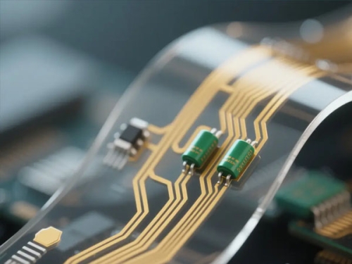

The Advanced Manufacturing Process of Flexible PCBs
Flexible Printed Circuits (FPCs) require highly precise engineering environments and sophisticated workflows. Below are the standard manufacturing standard operating procedures (SOP) for both double-sided and single-sided flexible PCBs.
1. Double-Sided FPC Manufacturing Process
Phase 1: Base Preparation & Via Hole Creation
Material Cutting →rightarrow→ Drilling →rightarrow→ PTH (Plated Through Hole) →rightarrow→ Panel Plating
Phase 2: Inner Layer Patterning (First Side)
Pretreatment →rightarrow→ Dry Film Lamination →rightarrow→ Alignment →rightarrow→ Exposure →rightarrow→ Development →rightarrow→ Pattern Plating →rightarrow→ Film Stripping
Phase 3: Outer Layer Patterning & Etching (Second Side)
Pretreatment →rightarrow→ Dry Film Lamination →rightarrow→ Alignment & Exposure →rightarrow→ Development →rightarrow→ Etching →rightarrow→ Film Stripping
Phase 4: Surface Protection & Finishing
Surface Treatment →rightarrow→ Coverlay Lamination →rightarrow→ Pressing →rightarrow→ Curing →rightarrow→ Surface Finishing (ENIG/Plating) →rightarrow→ Silkscreen Printing
Phase 5: Fabrication, Final Inspection & Shipping
Shearing →rightarrow→ Electrical Testing (E-Test) →rightarrow→ Punching & Die Cutting →rightarrow→ Final Inspection (FQC) →rightarrow→ Packaging →rightarrow→ Shipment
2. Single-Sided FPC Manufacturing Process
Step 1: Cutting →rightarrow→ Drilling →rightarrow→ Pretreatment
Step 2: Dry Film Lamination →rightarrow→ Alignment →rightarrow→ Exposure →rightarrow→ Development
Step 3: Etching →rightarrow→ Film Stripping →rightarrow→ Pretreatment
Step 4: Coverlay Lamination →rightarrow→ Pressing →rightarrow→ Curing
Step 5: Surface Finishing (ENIG/Plating) →rightarrow→ Silkscreen Printing →rightarrow→ Shearing
Step 6: Electrical Testing (E-Test) →rightarrow→ Punching & Outline Cutting rightarrow→ Final Inspection →rightarrow→ Packaging →rightarrow→ Shipment